Every time people think that Moore’s Law has reached its limit, scientists try to find a new solution to prolong its life again. Now materials science research efforts are looking to take the limits of Moore’s Law to the next level.
In a new paper published in the journal Nature, scientists at Tsinghua University in Shanghai say they have created the GATE pole on a graphene transistor with a width of just 0.34 nanometers – equivalent to equivalent to the width of a carbon atom.
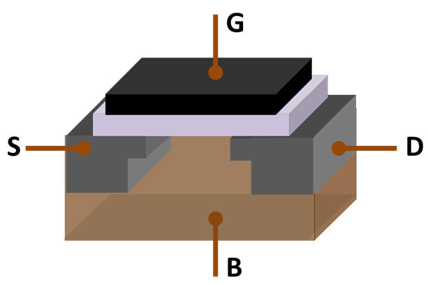
For transistors, this Gate pole is a very important component when it is used to control the current in and out of the Source and Drain terminals. Even this gate length – or the distance between the Source and Drain terminals – has been named for the chip manufacturing process – a metric that shows how advanced and advanced the chip is.

The basic components of the transistor: Gate terminal (G), Source terminal (S) and Drain terminal (D).
But from more recent processes (under 14nm and below), these numbers only have a marketing and identifier meaning when the process name no longer represents the GATE pole length. That’s because if shrinking to this size equals its process name, the limitations of material technology will damage that chip.
But in fact, many studies have narrowed this gap to 1nm and below. But this is the first time this distance has been narrowed to 0.34nm – about the size of a carbon atom – and this could be its final frontier. Study author Tian-Ling Ren said: “This could be the last node of Moore’s Law.”
Graphene Transistor
Although silicon is a suitable compound for chip production, when the GATE terminal length is reduced to less than 5nm, electrons tend to leak through the other terminals on the transistor. But in 2016, using carbon nanotubes with a 2D material called Molybdenum Di-Sulfide, the researchers created a 1nm long GATE pole. Despite having a higher resistance than silicon, this has helped Molybdenum Di-Sulfide bring the GATE terminal length on the transistor to a new limit.
Based on this research, scientists from Tsinghua University of China also selected Molybdenum DiSulfide as the material for the conduction channel and GATE electrode on the transistor. But instead of carbon nanotubes, the researchers used graphene sheets with a thickness of just 1nm.
Through a production method known as chemical vapor deposition, the scientists were able to sandwich a layer of graphene between two layers of insulators, aluminum oxide and silicon Di-oxide. The sheet is then etched to create a ladder-like shape and expose the edge of the graphene sheet in the vertical wall of the step. This exposed part forms a thin GATE pole about the size of a carbon atom.

Finally, the team added a layer of Hafnium Oxide to form a small space between the GATE electrode and the channel made of a layer of Molybdenum Di-Sulfide. They then added two more metal electrodes, above and below the top plate, to form the Source and Drain terminals for the new transistor.
Hard to come true in the near future
Despite reaching a distance that is almost unthinkable in the semiconductor world – 0.34nm – this work is just a proof-of-concept: a proof of the researchers’ hypothesis.
This approach is only suitable for manufacturing a very small number of transistors in the laboratory, but it is difficult to mass produce to form chips for your smartphone or laptop. Not to mention this approach, which mostly uses expensive materials for production, makes scaling up production a difficult challenge to overcome.
Even though the GATE gap on transistors has not yet been closed, silicon-based chip technology continues to achieve new strides in performance and energy efficiency. While FinFET-designed transistors have gradually reached their limit, new technologies such as chips with the new Gate-All-Around (GAA) design, promise to continue to maintain the momentum of efficiency. The power and effectiveness of Moore’s Law. More importantly, these technological advancements are already within reach, with new products coming over the next few years.
Refer to Singularityhub
