According to a recent report by the Zelenograd city government, the Russian government will provide 670 million rubles (about $8.5 million) to support research into new chip lithography technology.
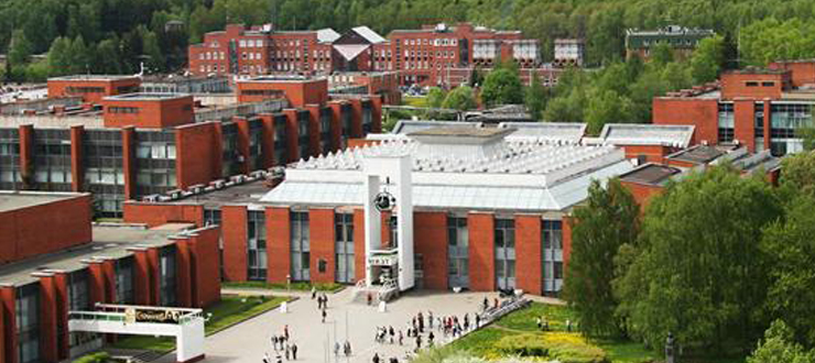
The Moscow Institute of Electronic Technology (MIET) is responsible for the proper use of this funding, in promoting the plan to develop a maskless photolithography based on X-ray synchronization technology and ( or) plasma source. The new type of device is expected to be able to process semiconductor wafers with sizes of 28nm, 16nm, or even smaller.
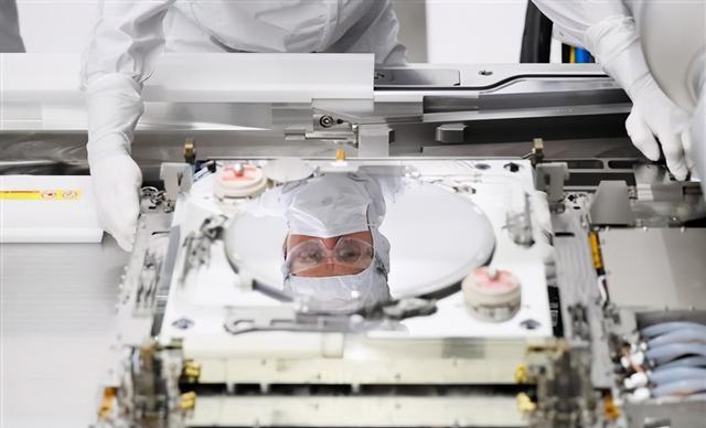
If you don’t know, basically, a light lithography system consists of a source of ultraviolet rays, this ultraviolet beam is amplified and then shined through a mask (photomask). The mask is a light shield, on which to print the details to be created, from which the detail will be printed on the variable contrast area. Through the converging lens, the shadows of the light beam converge to create microscopic details. This is considered the most advanced technology in photolithography today.

Moscow Institute of Electronic Technology (MIET).
Western sanctions are having a devastating effect on the Russian economy, not only in the markets of daily necessities and consumer electronics, but also semiconductors, which are very important to the industry. local industry as well as the military sector.
At the end of last month, the Russian government decided to provide some much-needed funding to many local research institutes, to develop the essential machinery for the “homegrown” semiconductor business. In addition, the country is also considering cooperation with China.
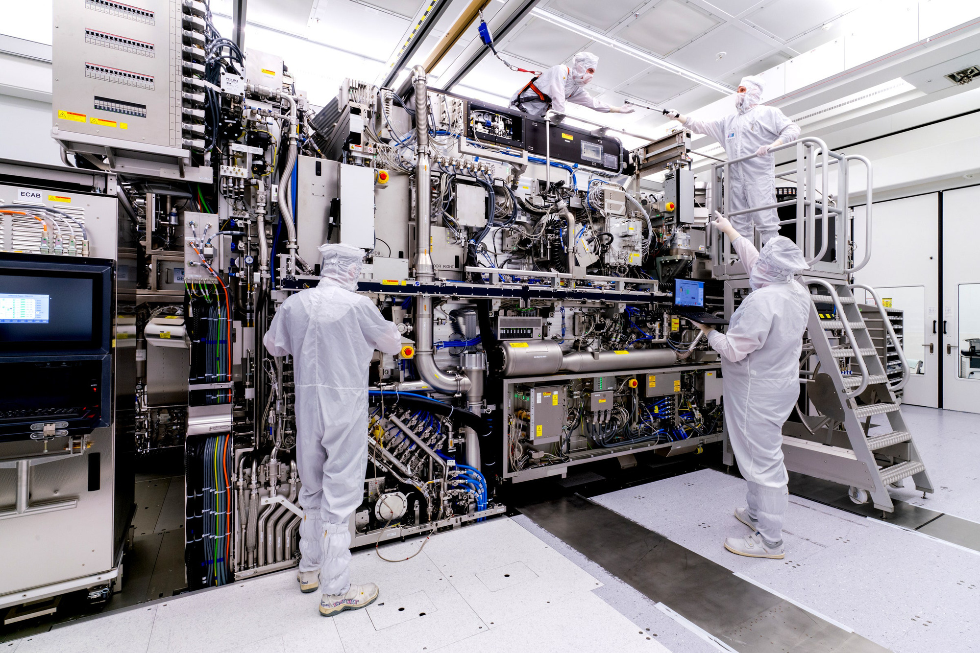
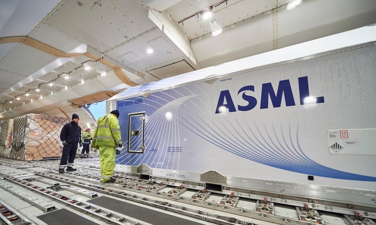
As for the semiconductor field, the Netherlands-based ASML company has long been the only supplier of EUV ultraviolet lithography machines. Large companies such as TSMC, Samsung and Intel are all customers of ASML, but the list of countries allowed to buy photolithography does not include Russia and China. This has hindered the development of the chip foundry industry of these two powers.

EUV lithography is now one of the indispensable equipment in advanced chip manufacturing, but have you ever wondered why this device is indispensable or substitute?
This issue concerns the so-called Union EUV LLC. In the early days of the semiconductor industry, to develop the photolithography standard, the U.S. Department of Energy led the creation of an alliance that included IBM, Intel, AMD, Motorola, and other technology companies, as well as three major laboratories are Lawrence Livermore, Sandia and Lawrence Berkeley. This alliance subsequently made a breakthrough in ultraviolet light technology and subsequently made ASML the main manufacturer of EUV lithography.
So, although the EUV lithography machine is on the outside a product of ASML, behind it is the backing of many Western technology companies.
Therefore, when researching the new photolithography machine, the Russian side chose X-rays, not ultraviolet (EUV) rays as the light source. The wavelength of ultraviolet light is 13.5nm, which can be used to manufacture advanced semiconductor processes of 7nm or less. The wavelength of X-rays ranges from 0.01 nm to 10 nm, and in theory it could also be used for photolithography with even more advanced processes. At the same time, another advantage of the X-ray lithography machine is that it will not need a mask, making it a practical solution in terms of cost and performance.

EUV lithography is the pinnacle of global collective technology, not just the fruit of a single manufacturer.
As a great power, Russia also has a wealth of technology, especially in X-ray and plasma. Now, jumping out of the EUV framework and choosing X-rays as the lithography breakthrough is seen as a practical option. At the same time, because of the shorter wavelength, X-rays are also capable of passing EUV lithography machines in the process of 1 nm or less.
But, the challenge for this choice is not small, the first is the supply chain issue of the industry. Why is EUV lithography hard to replace? Because behind 100,000 parts of this machine is the crystallization of many leading technology companies in the world, including light source system, optical lens system, dual workpiece system… Production The EUV lithography machine is today a complete industrial chain, with different companies responsible for creating each of the different precision parts.
X-ray lithography might indeed be theoretically possible, but without the support of an industrial production line, it would be difficult to produce a prototype, let alone build a prototype. mass production of this product. Not to mention even if it was created, the cost would be an astronomical number. As a result, the product costs will be greatly increased, and eventually lead to the failure of the whole plan.

But the Russians are very confident. MIET says it is not only refining its X-ray lithography scheme, but wants to delve deeper.
Nikolai Dyuzhev, field manager for Microsystems and Electronics at MIET said: “Our project is a one-of-a-kind project. No organization or country has ever performed maskless lithography on such a principle before.”
As planned, this project is expected to start in November this year. Before that, it will take time to finalize the technical specifications along with a feasibility study for a complete X-ray lithography prototype.
And, we will still have to wait at least 5 years for the testing process with this technology to start. Although the project is far from reality, it promises to play an important role for the global semiconductor manufacturing science.
Synthetic
